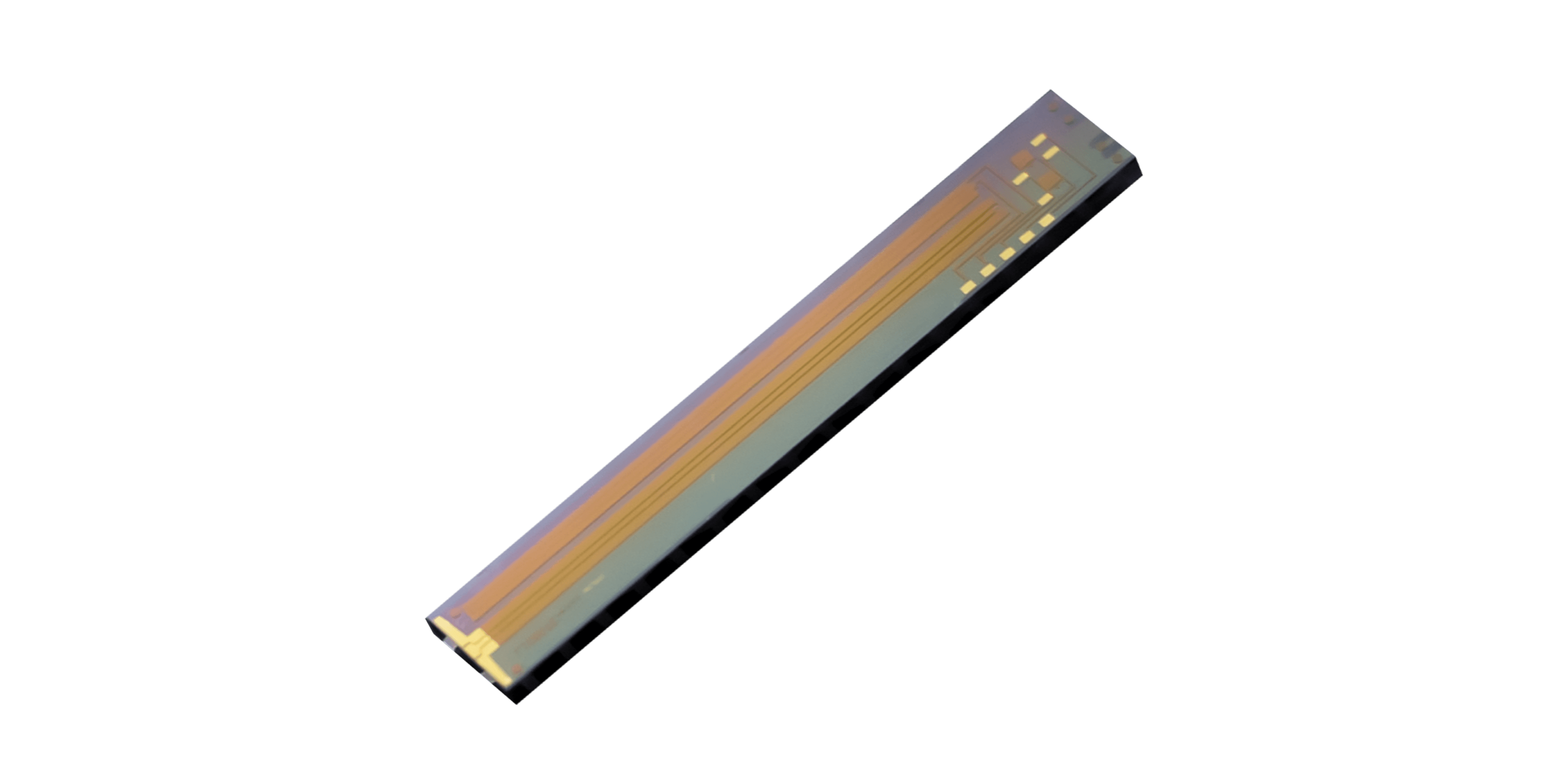
Specialized signal processing often begins in electronics, but many applications need the resulting waveform to travel, interact, or be measured in the optical domain. They use electro-optic conversion to transfer controlled amplitude and phase information onto light.
This allows high-frequency signals to benefit from optical bandwidth, low propagation loss, wavelength multiplexing, and immunity to electromagnetic pickup. The conversion step is not transparent. A modulator adds frequency response, nonlinearity, loss, bias behavior, and noise sensitivity that influence the waveform delivered to the next stage.
Consequently, they model the optical device as part of the signal-processing chain rather than a connector between two otherwise independent subsystems. Published TFLN chips cover intensity, IQ, and polarization-division-multiplexed functions from 70 to 110 GHz.
These formats can support data transmission, microwave photonics, waveform generation, testing, and sensing. They use the available figures to establish design ranges, while prototype measurements determine how the component behaves with their drivers, optical sources, receivers, and algorithms.
Optical Modulation Extends the Reach of Electronic Waveforms
An electro optic modulator maps an electrical voltage onto an optical property. Intensity devices vary transmitted power, phase devices shift optical phase, and IQ circuits control two orthogonal components for complex modulation.
This translation lets them create optical waveforms that encode data, synthesize sidebands, distribute microwave signals, or probe a system with precisely timed patterns.
With TFLN chips, the thin-film lithium-niobate waveguide and electrode geometry provide the physical interaction. Strong overlap between the RF field and optical mode can reduce required voltage, while traveling-wave electrodes extend response to high frequency.
The design still depends on impedance, velocity matching, termination, and package transitions, all of which can reshape the intended electrical waveform. Signal processing can also use polarization as an additional degree of freedom.
A polarization-division-multiplexed IQ circuit generates separate complex signals on two polarization states, increasing information capacity. For measurement applications, however, simpler intensity or phase functions may offer easier calibration. They choose the optical architecture according to the mathematical operation and acceptable control complexity.
Device Parameters Shape the Signal-Processing Burden
Bandwidth sets the frequency range over which an electro-optic modulator can reproduce a waveform with controlled amplitude and phase. A listed bare intensity die reaches 110 GHz, while a coherent PDMIQ device is specified at 70 GHz.
They examine the full response, group delay, and package contribution because a single cutoff value does not predict waveform fidelity. Drive voltage determines how demanding the interface is for the electronic amplifier or digital-to-analog converter. The bare die lists half-wave voltage below 3 V, whereas the coherent circuit uses a differential figure below 4.5 V.
When selecting TFLN chips, they calculate actual voltage swing, impedance loss, linearity, and power rather than comparing voltage numbers measured under different conventions. Optical loss affects signal-to-noise ratio and may increase laser or amplifier requirements.
The coherent device is listed below 7 dB insertion loss, and the bare die below 5 dB at its reference plane. Extinction ratio also influences residual carrier or amplitude contrast. They propagate these values through the receiver and processing model to estimate usable dynamic range.
Integration and Test Must Be Planned as One Workflow
Co-design begins with shared simulation data. The RF team supplies source impedance, output swing, package model, and waveform spectrum; the optical team contributes coupling, loss, bias behavior, and wavelength dependence; algorithm developers define error tolerance and compensation capability.
This exchange prevents an electro-optic modulator from being specified with assumptions that no adjacent subsystem can meet. They qualify TFLN chips using representative patterns and analog waveforms, both a network-analyzer sweep. Eye diagrams, error vector magnitude, spurious response, harmonic distortion, bias drift, and noise reveal different limitations.
Temperature and optical-power sweeps show whether calibration remains valid, while multi-unit testing distinguishes a stable operating window from a selected sample. Production planning must preserve traceability between chip data and final system behavior. They store wafer, die, package, driver, firmware, and calibration identifiers with test results.
If performance shifts, this record helps locate the source and supports focused corrective action. Clear change-control rules are equally important because a small process adjustment may alter high-frequency response or bias characteristics. Calibration headroom should remain visible in the processing architecture.
Compensation can correct predictable imperfections, but using many of its range during initial production leaves little allowance for aging or temperature. They set component limits so algorithms improve performance without becoming a substitute for stable hardware.
Specialized processing gains value from optical modulation when the conversion is treated quantitatively. They define the waveform that must emerge, allocate error and power budgets, and identify which impairments can be compensated without creating excessive complexity. That method keeps device selection connected to system outcomes rather than to isolated record specifications.
For commercial programs, a pilot chain should include the planned electronics, optical source, package, receiver, and processing software. Measurements from that chain can set realistic purchasing limits and calibration procedures. They also reveal whether additional bandwidth, lower voltage, or lower loss produces a meaningful improvement in the intended operating range.
Waveform quality depends on the modulator, driver, package, and measurement chain acting together. Testing Liobate chips in that shared environment allows linearity, stability, process control, and integration effort to be judged from the same evidence set.